
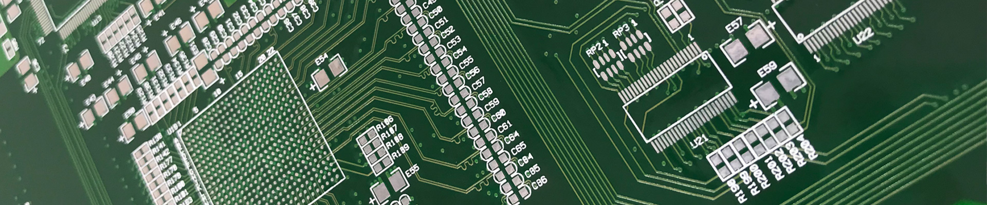
PCB CAPABILITIES
| Items | Manufacturing Capabilities | Remarks |
| Number of Layers | 1-40 layers | NA |
| Maximum PCB Size(Dimension) | 500x1100 mm | Any sizes beyond this dimension, please contact us. |
| Board Size Tolerance(Outline) | ±0.2mm/±0.5mm | ±0.2mm for CNC routing, and ±0.5mm for V-scoring. |
| Board Thickness | 0.4-2.4mm | 0.4, 0.6, 0.8, 1.0, 1.2, 1.6, 2.0, 2.4mm. Please contact us if your board exceeds these. |
| Board Thickness Tolerance(t≥1.0mm) | ±10% | Normally "+ Tolerance" will occur due to PCB processing steps such as electroless copper, solder mask and other types of finish on the surface. |
| Board Thickness Tolerance(t<1.0mm) | ±0.1mm | |
| Min Trace | 0.1mm/4mil | Min manufacturable trace is 4mil(0.1mm), strongly suggest to design trace above 6mil(0.15mm) to save cost. |
| Min Spacing | Min manufacturable spacing is 4mil(0.1mm), strongly suggest to design spacing above 6mil(0.15mm) to save cost. | |
| Outer Layer Copper Thickness | 1oz/2oz/3oz/4OZ or heavier | We make heavy copper PCB, as heavy as 30oz! |
| Inner Layer Copper Thickness | 1oz/1.5oz(35μm/50μm) | Inner copper weight as per customer's request for 4 and 6 layers. Please contact us if you need copper weight greater than 1.5oz. |
| Drill Sizes (CNC) | 0.2-6.3mm | Min drill size is 0.2mm, max drill is 6.3mm. Any holes greater than 6.3mm or smaller than 0.3mm will be subject to extra charges. |
| Min Width of Annular Ring | 0.15mm(6mil) | For pads with vias in the middle, Min width for Annular Ring is 0.15mm(6mil). |
| Finished Hole Diameter (CNC) | 0.2mm-6.2mm | The finished hole diameter will be smaller than size of drill bits because of copper plating in the hole barrels |
| Finished Hole Size Tolerance(CNC) | ±0.08mm | For example, if the drill size is 0.6mm, the finished hole diameter ranges from 0.52mm to 0.68mm will be considered acceptable. |
| Minimum Character Width(Legend) | 0.15mm | Characters of less than 0.15mm wide will be too narrow to be identifiable. |
| Minimum Character Height (Legend) | 0.8mm | Characters of less than 0.8mm high will be too small to be recognizable. |
| Character Width to Height Ratio (Legend) | 1:5 | In PCB silkscreen legends processing, 1:5 is the most suitable ratio |
| Minimum Diameter of Plated Half Holes | 0.6mm | Design Half-Holes greater than 0.6mm to ensure better connection between boards. |
| Surface Finishing | Lead free HAL,Gold/Silver Immersion,Hard Gold,OSP | NA |
| Solder Mask | Green, Blue, Red, White, Black, Matt black, Yellow, Purple, Pink | Green, Blue, Red, White, Black is standard offer, and other color need extra charge |
| Silkscreen | White, Black, None | No extra charge. |
| Panelization | V-scoring,Tab-routing,Tab-routing with Perforation (Stamp Holes) | Leave min clearance of 1.6mm between boards for break-routing. For V-score panelization, set the space between boards to be zero. |
